Facilities
Microfabrication Technology
Spin coating
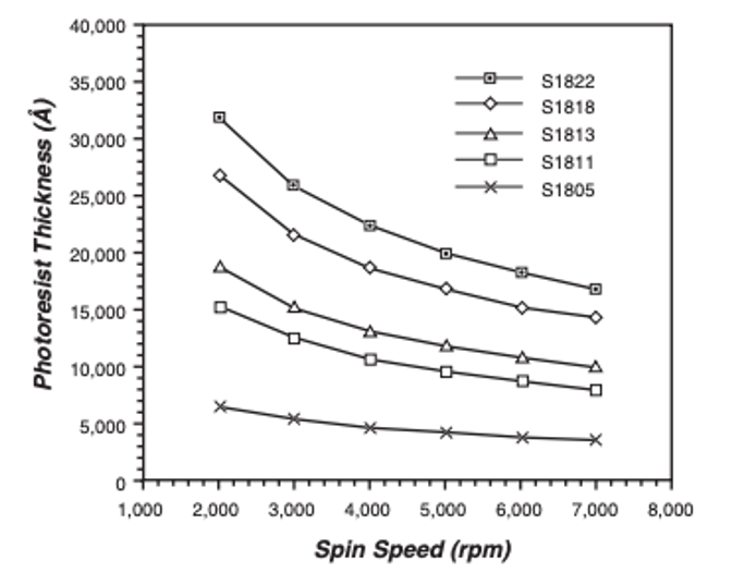
The spin coating process deposits a thin photoresist layer of controlled thickness on a substrate. The substrate, typically a silicon or glass wafer, is spin cast at a particular rotational speed, typically between 1000 rpm and 5000 rpm, for a selected time, typically 10s of seconds, which results in a particular thickness. The spin parameters are obtained from the data sheet supplied by manufacturer. An example spin curve for S1805 photoresist is shown below.
Step-by-Step illustration of Spin Coating Process
|
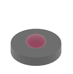
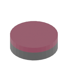
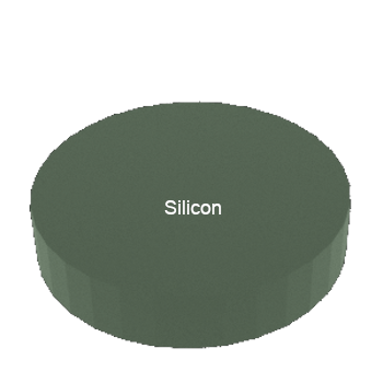
STEP 1: Start with substrate |
STEP 2: Drop few ml of photoresist on substrate |
|
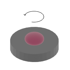
STEP 3: Spin substrate at selected rotation speed |
STEP 4: Uniform photoresist thin film on substrate |
Photolithography
The photolithography process uses UV light (g-line: 436 nm, h-line: 405 nm, and i-line: 365 nm) to pattern thin photoresist films. Photoresist is a light sensitive material that changes its chemical structure when exposed to UV light. The exposed photoresist is then removed in a chemical solution, known as a developer, to form the patterned photoresist layer. For contact photolithography, a physical mask, called as photomask, is used to control the exposure area on the substrate.
Step-by-Step Illustration of Contact Photolithography Process
|
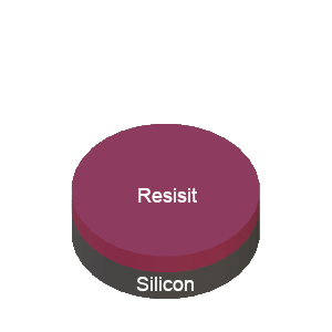
STEP 1: Starting with the substrate with uniform layer of photoresist |
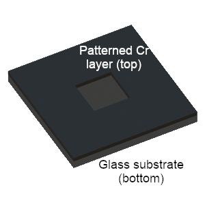
STEP 2: Fabricated photomask, typically Cr patterned on soda-lime glass |
|
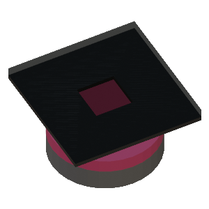
STEP 3: Photomask is placed in contact with the photoresist on the substrate. Collimated UV light above the glass mask (not shown) exposes the photoresist through the opening in the photomask |
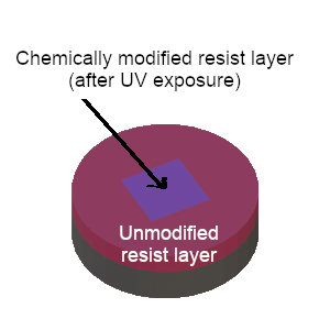
STEP 4: The resist exposed to UV light is chemically modified |
|
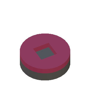
STEP 5(a): The substrate is placed in a developer solution. If the exposed photoresist is dissolved during development, the photoresist is called "positive" |
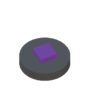
STEP 5(b): The substrate is placed in a developer solution. If the exposed photoresist remains after development, the photoresist is called "negative" |
Direct Write Photolithography Process
Direct write photolithography employs a focused UV laser beam to pattern photoresist on a substrate. In this case, the UV laser is rastered across the photoresist coated substrate according to the design requirements. The laser motion is controlled by a design drawn in mask layout software, for example AutoCAD. Direct write laser based exposure is often slower than the contact photolithography.
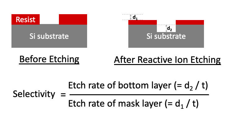
Etching: Dry and Wet
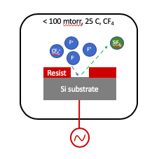
Reactive ion etching (RIE) is a dry etching process of transferring a pattern defined in a top mask layer, for example photoresist, to a second bottom layer, for example silicon, using a gas plasma, for example CF4 gas. The plasma is formed when electrons accelerated by a high electric field ionizes the gas molecules forming a "soup" of ions, neutral, and radicals. The ionized radicals are highly reactive and etch the exposed bottom layer. Etching occurs when reactant species, for example fluorine radicals, react with the bottom layer, for example silicon, that forms a byproduct, for example SiFx, which is volatile at room temperature and low pressure, for example 10s of mTorr. Additionally, physical etching occurs when plasma ions are propelled by the electric field striking the bottom layer.
Advanced RIE systems employ dual plasma sources to achieve faster etch rates, better control over the etch rate, selectivity, and side wall angle. For example, the IMSE RIE system uses an inductively coupled plasma (ICP) source in the top part of the chamber and a second plasma source at the substrate.
Ideally, a selected RIE etch process/chemistry will minimally etch the mask layer and will selectively remove the bottom layer. However, in reality the top mask layer is also etched. Plasma chemistry is selected to minimize the etch rate of the top mask layer and maximize the etch rate of the second bottom layer. Selectivity is often used to define the ratio of etch rates of the two layers. A "good" etch has a selectivity >> 1.
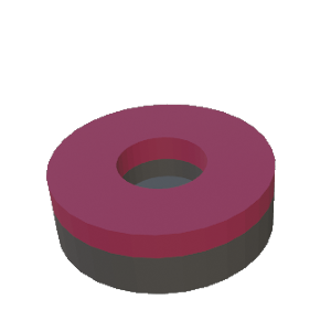
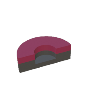
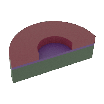
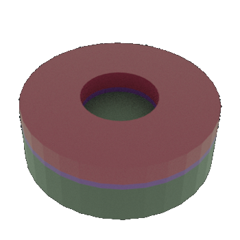
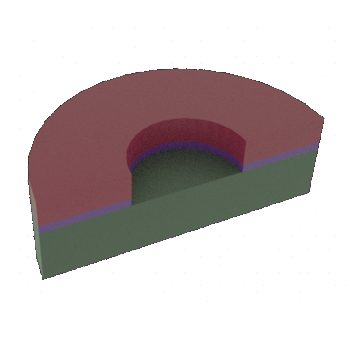
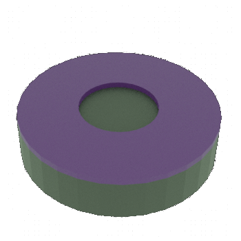
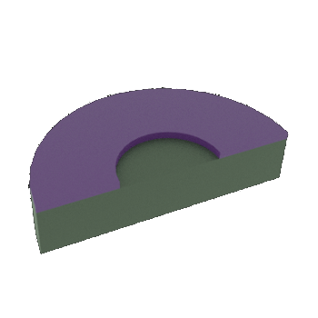
Step-by-Step Illustration of Etching Process
|
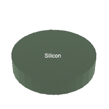
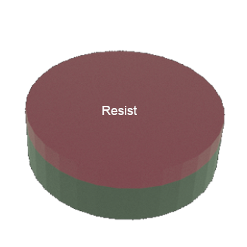
STEP 1a: Starting substrate with photoresist on top surface |
STEP 1b: Cross-sectional view of Step 1a |
|
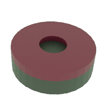
STEP 2a: Pattern photoresist using photolithography process |
STEP 2b: Cross-sectional view of Step 2a |
|
STEP 3a: After substrate is etched |
STEP 3b: Cross-sectional view of Step 3a |

Comparison of Dry and Wet Etching
The major disadvantage of wet etching is the loss of critical dimensions due to the isotropic nature of the wet etch process. For example, a 5 micron wide trench patterned in photoresist may turn out to be 10 microns wide. Dry etching enables more anisotropic etching and smaller critical dimensions.
Limitations of RIE Process
Certain materials, such as gold, do not easily form etch byproducts with sufficient vapor pressure, and hence cannot be easily etched. Metal etch processes can also leave residue in parts of the etching chamber. These residues can cause yield issues when etching other materials (such as SiO2). Therefore, the IMSE Micro Nano Fab limits the materials allowed in the Oxford RIE.
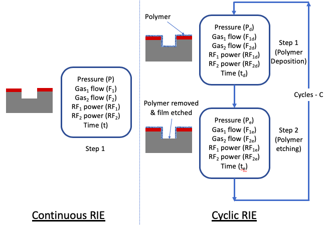
Deep Si RIE Etch Process
The continuous RIE process, explained above, is typically used to etch thin films with thickness less than a few microns. Etching thicker layers is difficult to maintain high selectivity and vertical sidewalls. The deep RIE (DRIE) silicon process overcomes this limitation by using a two-step cyclic process where one step is used to deposit a thin polymer film using a C4F8 gas, and the second step is used to remove the polymer and etch silicon at the bottom of the etched structure using a SF6 gas. A pair of two steps constitutes 1 cycle and is repeated for a number of cycles to get the desired etch depth. Repeated processes leads to additional roughness on the sidewalls, which is called scalloped sidewall. This cyclical etch process is called the Bosch process. Typically, this process is used to partially etch the silicon substrate with thickness > 100 microns, and often to completely through the silicon substrate.
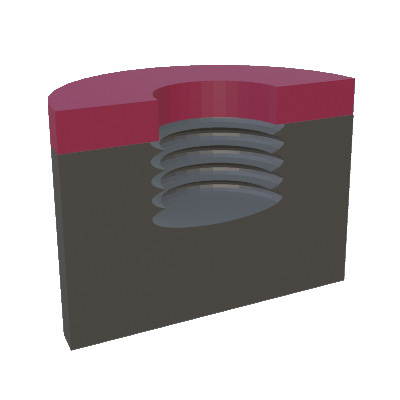 Formation of scallops during the DRIE process
Physical vapor deposition: Sputtering
Physical vapor deposition (PVD) by sputtering is enabled with a high electrical field around source material, or target. The electrical field creates a plasma and energetic ions propelled to the target remove material atoms by physical sputtering. The sputtered material subsequently deposits on the substrate.
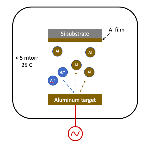
The plasma source can be generated by either a RF or DC source. Typically, a DC source is used for an electrically conducting target such as a metal, and a RF source is used for insulator target material, such as SiO2. Argon is the primary source gas, and in certain cases, oxygen can be mixed with Ar to deposit oxide forms of the target.
Step-by-Step illustration of Sputtering Deposition Process
|
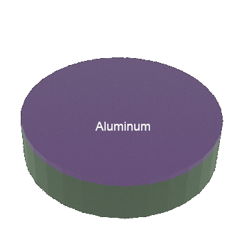
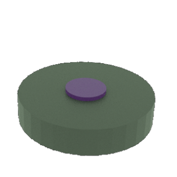
STEP 1: Starting substrate |
STEP 2: Substrate with Al thin film |
Physical vapor deposition: Evaporation
Thin-film electron-beam evaporation deposition uses an electron beam to heat the target material. The electron beam is generated by thermionic or field emission. The electron beam is accelerated using controlled electric and magnetic fields, and manipulated to strike the target material in the crucible. Typically, the material is used in small pellet form, for example 1 mm size, and placed in a crucible, for example boron nitride ceramic. The crucible temperature is controlled to prevent excessive heating. The crucible material is selected such that it has a higher melting point than the target material. The evaporated material is then deposited on the substrate. A large mean free path in vacuum ensures the evaporated material is deposited on the substrate.
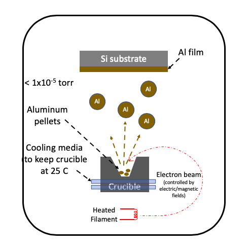
Comparison with Thermal Evaporation
The thermal evaporation process heats the boat to a very high temperature, and hence the boat material can potentially contaminate the deposited film. However, in the electron-beam deposition process, only the material of interest is heated. The boat is kept at room temperature at all times, and which gives a very high purity thin film. Electron-beam evaporation can also deposit metals which may form alloys at high temperature with boat. For example, platinum can be deposited by electron-beam evaporation and not thermal evaporation.
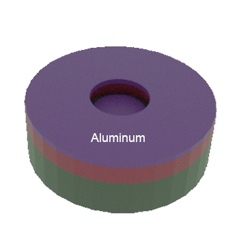
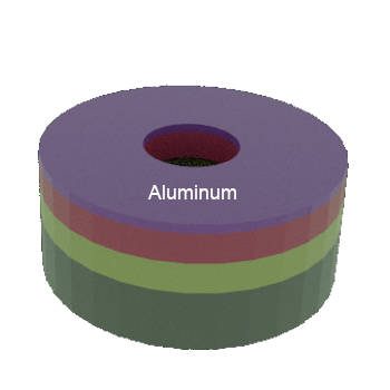
Step-by-Step Illustration of Metal Deposition Process
|
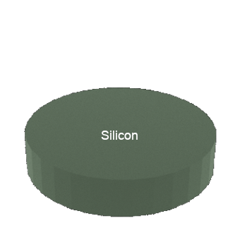
STEP 1: Starting substrate |
STEP 2: Substrate with Al thin film |
Thin film patterning
Thin-film patterning is a process of patterning thin films using a combination of deposition, metal removal, and photolithography. Two widely used methods are:
- Subtractive Transfer: Photoresist layer is patterned on top of the thin film. The exposed film is then etched, and followed by removal of the photoresist.
- Additive Transfer (lift-off method): Thin film is deposited over patterned photoresist layer. The photoresist layer is then removed (or lifted off) to give patterned thin film. A single layer of photoresist may be replaced with two layers of photoresist for better repeatability.
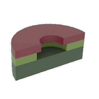
Step-by-Step Illustration of Thin-Film Deposition using Subtractive Transfer Process
|
STEP 1: Starting substrate |
STEP 2: Substrate with Al thin film |
|
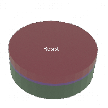
STEP 3: Al/substrate with photoresist thin film |
|
|
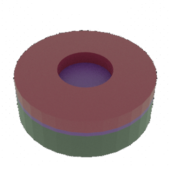
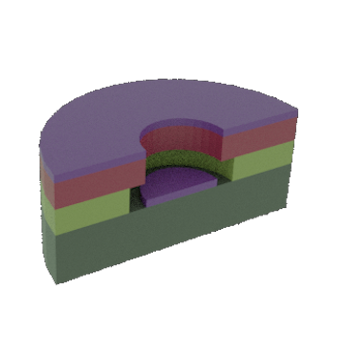
STEP 4a: Al/substrate with patterned photoresist thin film |
STEP 4b: Cross-sectional view of 4a |
|
STEP 5a: Exposed Al removed by wet etching |
STEP 5b: Cross-sectional view of 5a (Undercut in Al layer not shown) |
|
STEP 6a: Patterned Al layer after removal of photoresist layer |
STEP 6b: Cross-sectional view of 6a |
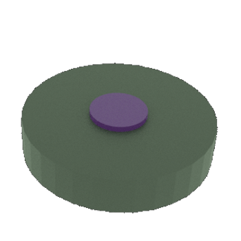
Step-by-Step Illustration of Deposition using Additive Transfer Process with Single Photoresist Layer
Typically, a negative photoresist layer is used to give a negative profile which helps in the lift-off process.
|
STEP 1: Starting substrate |
STEP 2: Substrate with photoresist layer |
|
STEP 3a: Patterned photoresist layer |
STEP 3b: Cross-sectional view of 3a. NOTE: negative profile in the photoresist layer |
|
STEP 4a: After Al deposition |
STEP 4b: Cross-sectional view of 4a |
|
STEP 5a: Patterned Al layer after photoresist layer is "lifted off" |
STEP 5b: Cross-sectional view of 5a |
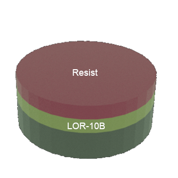
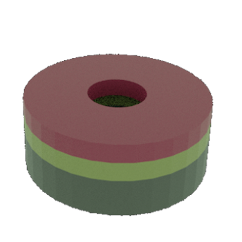
Step-by-Step Illustration of Deposition using Additive Transfer Process with Two-Layer Photoresist
In the two layer process, a first photoresist layer, for example LOR-10B, and second layer is positive, or negative, photoresist. Developer solution used for second layer photoresist also removes the exposed LOR-10B layer.
|
STEP 1: Starting substrate |
STEP 2: Substrate with two layers of photoresist |
|
STEP 3a: Patterned photoresist layers |
STEP 3b: Cross-sectional view of 3a |
|
STEP 4a: After Al deposition |
STEP 4b: Cross-sectional view of 4a. NOTE: The LOR-10B layer dissolves faster than the top photoresist layer. |
|
STEP 5a: Patterned Al layer after photoresist layers are "lifted off" |
STEP 5b: Cross-sectional view of 5 |
Thermal oxidation
Thermal oxidation is employed to oxidize silicon using dry oxygen (dry oxidation) or water steam (wet oxidation) at high temperature, for example 1100oC. At high temperatures, oxygen reacts with silicon to form silicon dioxide (SiO2). As silicon is oxidizing, oxygen reaching the silicon surface is reduced and controlled by diffusion. Hence, the oxidation rate decreases with time.
Chemical vapor deposition
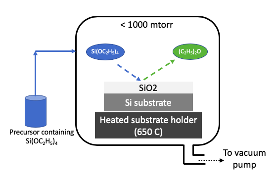
Chemical Vapor Deposition (CVD) uses one or more volatile precursors to deposit high quality thin films on substrates. Substrate is heated to a desired temperature to create a chemical reaction on the substrate. For example, a tetraethylorthosilicate precursor in vapor form will decompose at a high temperature on a substrate to deposit a silicon dioxide thin film. The CVD process is performed in vacuum to obtain uniform deposition and high purity thin films.
Many standard precursors are available today that can deposit metals, silicon oxide, silicon, and silicon nitride by the CVD process. The precursor must be volatile, leave no impurity in deposited films, and give desired film properties, such as uniformity, electrical resistance, and surface roughness. All byproducts from CVD surface reactions should be volatile and easily removable in vacuum. Precursors should not react among each other in vapor form, and only react at high temperature maintained at the substrate.
Plasma enhanced chemical vapor deposition (PECVD)
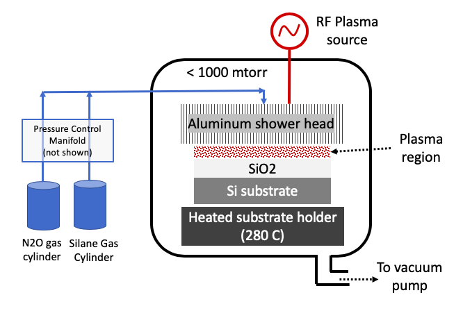
Plasma Enhanced Chemical Vapor Deposition (PECVD) uses plasma of ionized species to break one or more stable volatile precursors to deposit high quality thin films on desired substrates. Plasma is created by applying high RF electric field around the area near the substrate. Plasma is widely known to break stable molecules that would have otherwise taken much higher thermal energy (or temperature) to break. These reactive plasma species deposit on heated substrate to deposit thin film of interest. Unlike CVD which uses only thermal energy on substrate, PECVD process uses both energy from plasma and thermal energy on substrate to achieve desired chemical reaction for thin film growth. For example, silane (SiH4) and nitrous oxide (N2O) can deposit SiO2 films at 280oC using the PECVD process.
Many standard precursors are available today that can deposit metals, silicon oxide, silicon, silicon nitride, etc by the PECVD process. The precusor must be volatile, leaves no impurity in deposited films, and give desired film properties, such as uniformity, electrical resistance, roughness. All byproducts from PECVD surface reaction should be volatile and easily removable in vacuum.
Atomic layer deposition (ALD)
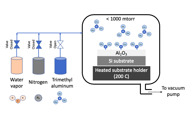
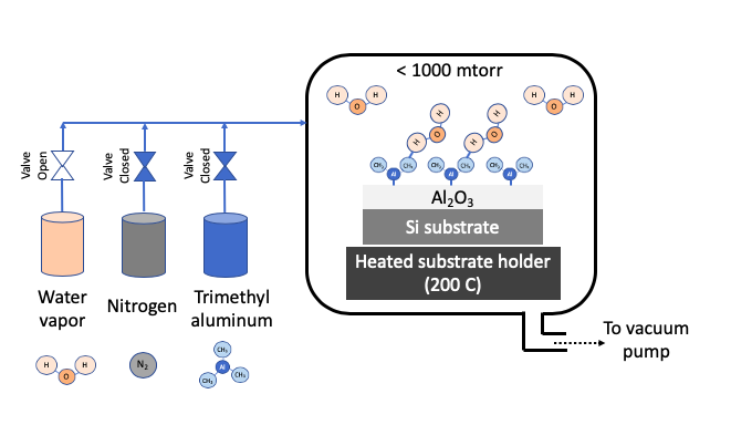
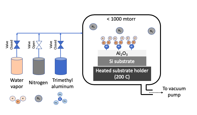
Atomic layer deposition (ALD) uses one or more volatile precursors or gases to deposit high quality thin films on desired substrates with precision controlled at angstrom length scale. Unlike a CVD process which uses continuous flow of gases, the ALD process introduces precursors in the chamber in a sequential manner. Sequential approach and chemistry selection ensures that each precursor only forms a single monolayer at a time. For example, Al2O3 is deposition by first flowing a trimethyl aluminum precursor, then purging chamber with nitrogen, then flowing water vapor as second precursor, and then purging with nitrogen again. These four steps constitute 1 ALD cycle, and gives a growth rate of about 1 Angstron per cycle. A cycle is repeated to get the desired film thickness. A nitrogen purge between the steps of ALD cycle prevents an undesired reaction in vapor phase. The ALD process can deposit films in a highly uniform manner in any size or shape especially when repeatability is critical at angstrom length scale. ALD precursors are carefully selected to foster desired ALD chemistry on heated substrate. Substrate is typically heated to a desired temperature (100 - 350oC) to create chemical reaction on substrates. ALD process is carried out in vacuum to obtain uniform deposition and high purity films.
Many standard precursors are available today that can deposit metals, metal oxides, silicon oxide, etc by ALD process. The precusor must be volatile, leave no impurity in deposited films, and give desired film properties, such as uniformity, electrical resistance, and surface roughness. All byproducts from ALD surface reaction should be volatile and easily removable in vacuum. Precursors should not react among each other in vapor form, and only react at high temperature maintained at substrate.
Step-by-Step Illustration of Steps in 1 ALD Cycle
|
STEP 1: Passivate surface with Precursor 1 (trimethyl aluminum) |
STEP 2: Remove excess Precursor 1 with nitrogen purge |
|
STEP 3: Introduce Precursor 2 (water vapor) to complete surface reaction |
STEP 4: Remove excess Precursor 2 with nitrogen purge |

Thin film metrology
Estimating film growth characteristics, such as deposition rate, surface roughness, and stochiometry, is critical for device microfabrication. The IMSE Micro Nano Fab and IMSE Materials Characterization facility provide a number of instruments, including optical microscopes, profilometer, ellipsometer, scanning electron microscope (SEM), atomic force microscope (AFM), and in situ quartz crystal microbalance (QCM) for quantitative thin-film measurements.
- Optical microscope: Measure the critical dimension width
- Profilometer: Measure the thin film height as long as step edge is available. Profilometers can also be used to estimate roughness of etched films.
- Ellipsometer: Measure the film thickness and optical constants of transparent materials deposited on silicon, glass, and sapphire substrates.
- Scanning electron microscope: Employs electrons to image sub-micron surface structures
- Atomic force microscope: Employs scanning nanomechanical probes to image sub-micron structures
- In situ QCM sensor: Measure the thickness deposited on substrate in real-time. The sensor must be calibrated using another metrology, for example, a profilometer.